當(dāng)前位置:首頁 > 產(chǎn)品中心 > 二維材料 > 硫化物晶體 > TiS2 二硫化鈦晶體 (Titanium Disulfide)


簡要描述:Our TiS2 crystals are stabilized in 1T ohase (semimetallic phase). They are grown using two different techniques through chemical vapor transport (CVT) or flux zone growth (see description of these tw
 更新時(shí)間:2024-06-02
 產(chǎn)品型號:
  廠商性質(zhì):生產(chǎn)廠家
 訪 問 量:810
相關(guān)文章
Related Articles詳細(xì)介紹
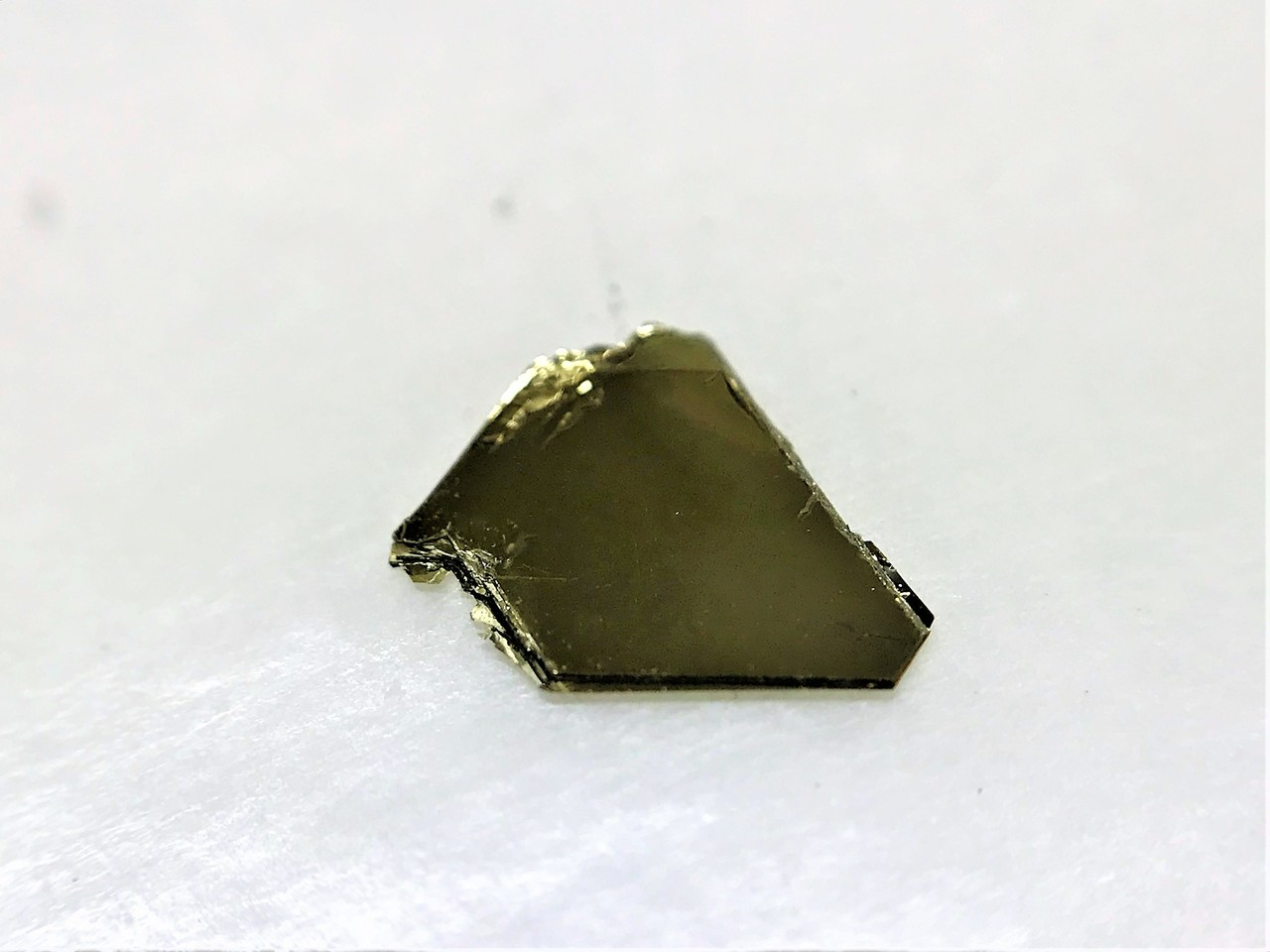
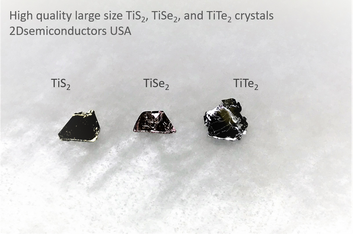
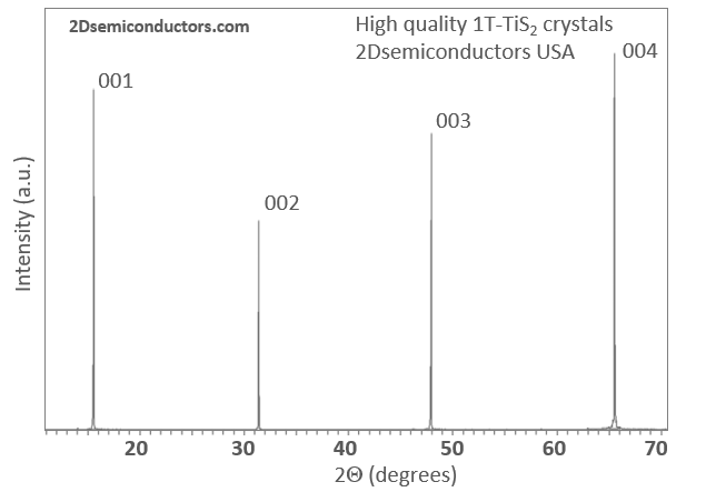
Our TiS2 crystals are stabilized in 1T ohase (semimetallic phase). They are grown using two different techniques through chemical vapor transport (CVT) or flux zone growth (see description of these two methods below). These crystals are treated as gold standards in 2D materials field owing to perfected electronic behavior with guaranteed phase transition and semimetallic responses. Our TiS2 crystals are notoriously known low impurity resistance (zero temperature resistance), high carrier mobility, extremely clean and sharp XRD peaks, and negligible amount of defects (see published results as well as CVT vs. Flux based methods below ). Our TiS2 crystals are large in size and ready for exfoliation without any preparation.
Properties of vdW TiS2 crystals

Growth method matters> Flux zone or CVT growth method? Contamination of halides and point defects in layered crystals are well known cause for their reduced electronic mobility, reduced anisotropic response, poor e-h recombination, low-PL emission, and lower optical absorption. Flux zone technique is a halide free technique used for synthesizing truly semiconductor grade vdW crystals. This method distinguishes itself from chemical vapor transport (CVT) technique in the following regard: CVT is a quick (~2 weeks) growth method but exhibits poor crystalline quality and the defect concentration reaches to 1E11 to 1E12 cm-2 range. In contrast, flux method takes long (~3 months) growth time, but ensures slow crystallization for perfect atomic structuring, and impurity free crystal growth with defect concentration as low as 1E9 - 1E10 cm-2. During check out just state which type of growth process is preferred. Unless otherwise stated, 2Dsemiconductors ships Flux zone crystals as a default choice.


產(chǎn)品咨詢
掃一掃以下二維碼了解更多信息

銷售微信咨詢

網(wǎng)站二維碼